VNA Assembling |
| Home | Projects | Tech Info | Media | Links | Contact | Store |
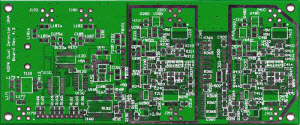
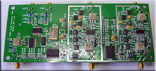
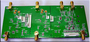
The bare dual detector v4.3 main board. |
|
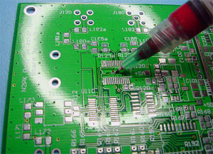
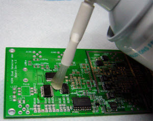
Surface mount adhesive heat curable is applied for holding ICs in place during soldering operation.
|
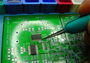
Chips are gently placed. |
|||
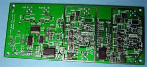
Board ready "to cook". |
|
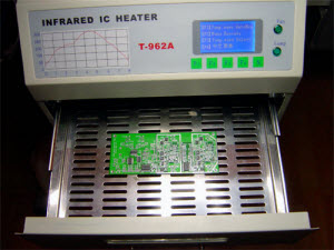
Board goes to the oven to cure the adhesive |
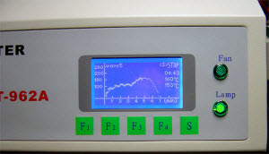
The computer controlled oven is progammed for cure operation. |
|||
After bake the board is cleaned. |
|
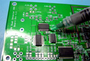
Solder paste is applied. |
Remaining oven solderable SMD components are placed on board. |
|||
The board goes back to the oven. It is progammed for reflow soldering. |
|
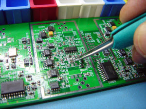
Next, components on top side, connectors, transformers and master oscillator are soldered at hand. |
Finished bottom side |
|||
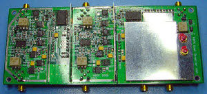
Screen walls among detectors and DDS sections. |
|
|
|
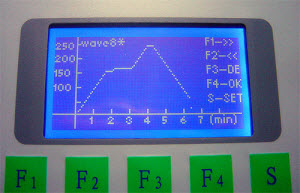
Multiple tests are conducted along the wiring stage.
|

|
|
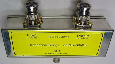
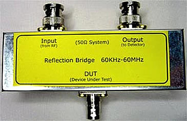
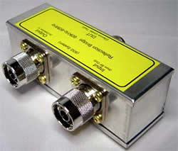
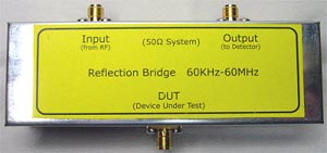
| Measurement bridge assembly details | ||||||
 |
 |
 |
||||
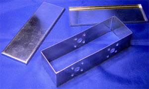
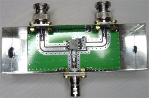
The measurement impedance bridge is mounted on a 110x36x30mm (4.331x1.417x1.181in) 0.5mm tin plate enclosure, providing more efficiency Faraday screening to electric and magnetic fields that aluminium ones.
|
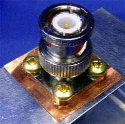
A thin copper sheet is placed between BNC connectors and box walls to seal any RF leakage. The excess of copper is cut after fixing connectors. To improve ground connectivity Brass Machine Phillips Pan Head Screws are used. |
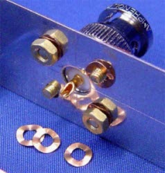
Copper Beryllium alloy crinkle washers and brass screws and nuts are used to set firmly the connectors. |
||||
 |
 |
 |
||||
The bridge PCB ground plane are soldered to box walls using Ag/Cu/Sn alloy. Transformer is original Mini-Circuits. Bridge resistors are precision 0.1% Connectors match with customer preferences. |
 |
 |
|
|
| Home | Projects | Tech Info | Media | Links | Contact | Store |